ELECTRONIC SYSTEM DESIGN FACILITY
Department of Electronics and Communication Engineering has the facility for the manufacturing of Electronic System in PCB from initial idea to final circuit process.
PCB facbrication facility
Component assembly facility
Testing and Inspection facility
Electronic ciruit designing software facilit
Prototying facilities
-

IDEA
-
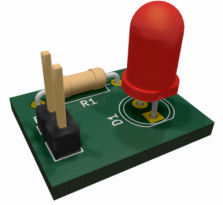
Design the circuit using software
-
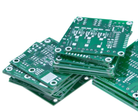
Fabricate a PCB using additive /subtractive technology
-
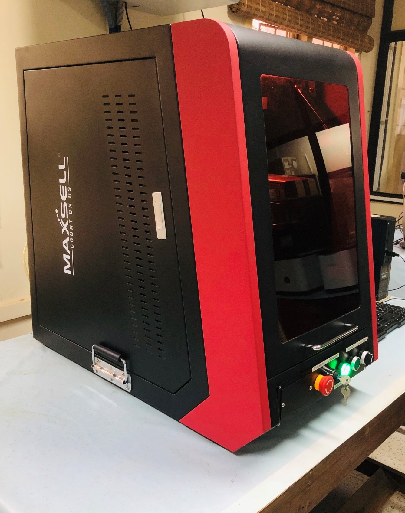
Use LASER machine to mark legend/silk screen
-

Use bot-factory/voltera (Silver nano particle technology) for multilayer
-
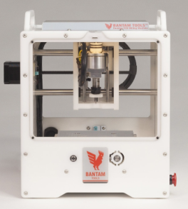
Use CNC bantam tools milling machine for through hole drilling
-
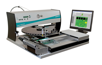
Assemble SMD components using PICK & PLACE machine
-

Solder through hole components using wave soldering machine
-
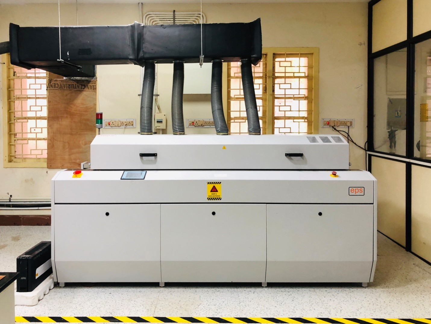
Solder SMD components using Reflow Oven machine
-

Use plotbot plus machine for outer case design
-

For embedded/memory programming use universal programmers
-

Finally test functionality of the product

